
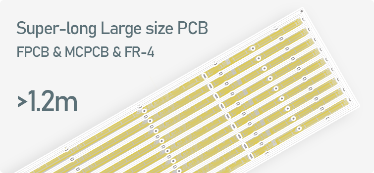

Multilayer PCB


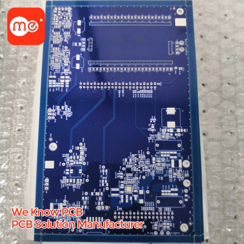


Immersion Tin 8L 2/1/1/1/1/1/1/1/2Oz PCB
Item No.: FR4-08
FR-4 94-V0
Blue SolderMask Immersion Tin
8L Multi-layer PCB
Blue SolderMask Immersion Tin
8L Multi-layer PCB
Description
Immersion Tin 8L 2/1/1/1/1/1/1/1/2Oz PCB
Hello everyone! Today, MeidearPCB will introduce to you what is the PCB Immersion Tin Process, what are its characteristics and what is its process flow?
First, let's introduce the Immersion Tin process of PCB:
PCB tin deposition process is specially designed to facilitate SMT and chip packaging. Tin metal coating is deposited chemically on the copper surface. It is a new green and environmental protection process to replace the Pb Sn alloy coating process. It has been widely used in the surface treatment of electronic products (such as circuit boards, electronic devices), hardware, decorations and so on.
There are two commonly used processes for printed circuit boards: HASL and Immersion Tin.
HASL is mainly to directly invade the PCB into the molten tin slurry. After hot air leveling, a dense tin layer with a thickness of 1um-40um will be formed on the copper surface of PCB.
Immersion Tin mainly uses displacement reaction to form a very thin tin layer on the surface of PCB. The thickness of tin layer is about 0.8um-1.2um. Tin deposition process is more commonly used in circuit board surface treatment process.
Both HASL-LF and Immersion Tin processes are a surface treatment method to meet the requirements of lead-free welding for PCB.
PCB Immersion Tin Processes Line
Special customized tin Immersion Tin circuit board Manufacturer | MeidearPCB
www.meidearpcb.com
mkt@me-pcb.com
If you need help or learn more information, please contact us freely.
Difference
Process flow: tin spraying, pretreatment - tin spraying - testing - forming - appearance inspection; Tin deposition, test - chemical treatment - tin deposition - forming - appearance inspection
Process principle: tin spraying is mainly to directly invade the PCB into the molten tin slurry. After hot air leveling, a dense tin layer will be formed on the copper surface of PCB. Tin deposition mainly uses displacement reaction to form a very thin tin layer on the surface of PCB.
Physical properties: tin spraying, the thickness of tin layer is about 1um-40um, the surface structure is dense, the hardness is large, and it is not easy to scratch; Tin spraying has only pure tin in the production process, so the surface is easy to clean, it can be stored for one year at normal temperature, and it is not easy to have the problem of surface discoloration during welding; The thickness of tin is about 0.8um-1.2um, the surface structure is loose and the hardness is small, which is easy to cause surface scratch; Tin deposition is a complex chemical reaction with many chemicals, so it is not easy to clean, and the liquid medicine is easy to remain on the surface, resulting in the problem of heterochromaticity in welding. The storage time is short, and it can be stored for three months at normal temperature. If it takes a long time, it will change color;
Appearance features: tin spraying, bright and beautiful surface; Sink tin, the surface is light white, matte and easy to change color.

Characteristics of Immersion Tin process
1. It still has excellent solderability after baking for 4 hours under 155 (equivalent to one year), or after 8 days of high temperature and high humidity test (45, relative humidity 93%), or after three reflow soldering;
2. The tin deposit layer is smooth, flat and dense, which is more difficult to form copper tin metal intermetallic compound than electroplating tin, and Wuxi must;
3. The thickness of tin deposit layer can reach 0.8-1.5 μ m. It can withstand multiple lead-free welding impact;
4. The solution is stable and the process is simple. It can be used continuously through analysis and supplement without cylinder replacement;
5. It is suitable for both vertical and horizontal processes;
6. The cost of tin deposition is much lower than that of nickel gold deposition, which is equivalent to that of hot air leveling;
7. It has obvious technical advantages for tin sprayed high-density boards that are easy to short circuit, and is suitable for hard and flexible boards of thin wire high-density IC packaging;
8. Suitable for surface mount (SMT) or press fit installation process;
9. Lead free, fluorine-free, no pollution to the environment, and free recovery of waste liquid.
Hello everyone! Today, MeidearPCB will introduce to you what is the PCB Immersion Tin Process, what are its characteristics and what is its process flow?
First, let's introduce the Immersion Tin process of PCB:
PCB tin deposition process is specially designed to facilitate SMT and chip packaging. Tin metal coating is deposited chemically on the copper surface. It is a new green and environmental protection process to replace the Pb Sn alloy coating process. It has been widely used in the surface treatment of electronic products (such as circuit boards, electronic devices), hardware, decorations and so on.
There are two commonly used processes for printed circuit boards: HASL and Immersion Tin.
HASL is mainly to directly invade the PCB into the molten tin slurry. After hot air leveling, a dense tin layer with a thickness of 1um-40um will be formed on the copper surface of PCB.
Immersion Tin mainly uses displacement reaction to form a very thin tin layer on the surface of PCB. The thickness of tin layer is about 0.8um-1.2um. Tin deposition process is more commonly used in circuit board surface treatment process.
Both HASL-LF and Immersion Tin processes are a surface treatment method to meet the requirements of lead-free welding for PCB.

PCB Immersion Tin Processes Line
Special customized tin Immersion Tin circuit board Manufacturer | MeidearPCB
www.meidearpcb.com
mkt@me-pcb.com
If you need help or learn more information, please contact us freely.
Difference
Process flow: tin spraying, pretreatment - tin spraying - testing - forming - appearance inspection; Tin deposition, test - chemical treatment - tin deposition - forming - appearance inspection
Process principle: tin spraying is mainly to directly invade the PCB into the molten tin slurry. After hot air leveling, a dense tin layer will be formed on the copper surface of PCB. Tin deposition mainly uses displacement reaction to form a very thin tin layer on the surface of PCB.
Physical properties: tin spraying, the thickness of tin layer is about 1um-40um, the surface structure is dense, the hardness is large, and it is not easy to scratch; Tin spraying has only pure tin in the production process, so the surface is easy to clean, it can be stored for one year at normal temperature, and it is not easy to have the problem of surface discoloration during welding; The thickness of tin is about 0.8um-1.2um, the surface structure is loose and the hardness is small, which is easy to cause surface scratch; Tin deposition is a complex chemical reaction with many chemicals, so it is not easy to clean, and the liquid medicine is easy to remain on the surface, resulting in the problem of heterochromaticity in welding. The storage time is short, and it can be stored for three months at normal temperature. If it takes a long time, it will change color;
Appearance features: tin spraying, bright and beautiful surface; Sink tin, the surface is light white, matte and easy to change color.

Characteristics of Immersion Tin process
1. It still has excellent solderability after baking for 4 hours under 155 (equivalent to one year), or after 8 days of high temperature and high humidity test (45, relative humidity 93%), or after three reflow soldering;
2. The tin deposit layer is smooth, flat and dense, which is more difficult to form copper tin metal intermetallic compound than electroplating tin, and Wuxi must;
3. The thickness of tin deposit layer can reach 0.8-1.5 μ m. It can withstand multiple lead-free welding impact;
4. The solution is stable and the process is simple. It can be used continuously through analysis and supplement without cylinder replacement;
5. It is suitable for both vertical and horizontal processes;
6. The cost of tin deposition is much lower than that of nickel gold deposition, which is equivalent to that of hot air leveling;
7. It has obvious technical advantages for tin sprayed high-density boards that are easy to short circuit, and is suitable for hard and flexible boards of thin wire high-density IC packaging;
8. Suitable for surface mount (SMT) or press fit installation process;
9. Lead free, fluorine-free, no pollution to the environment, and free recovery of waste liquid.